- 您现在的位置:买卖IC网 > Sheet目录346 > NCP5010FCT1G (ON Semiconductor)IC LED DRVR WHT BCKLT 8-FLIPCHIP
NCP5010
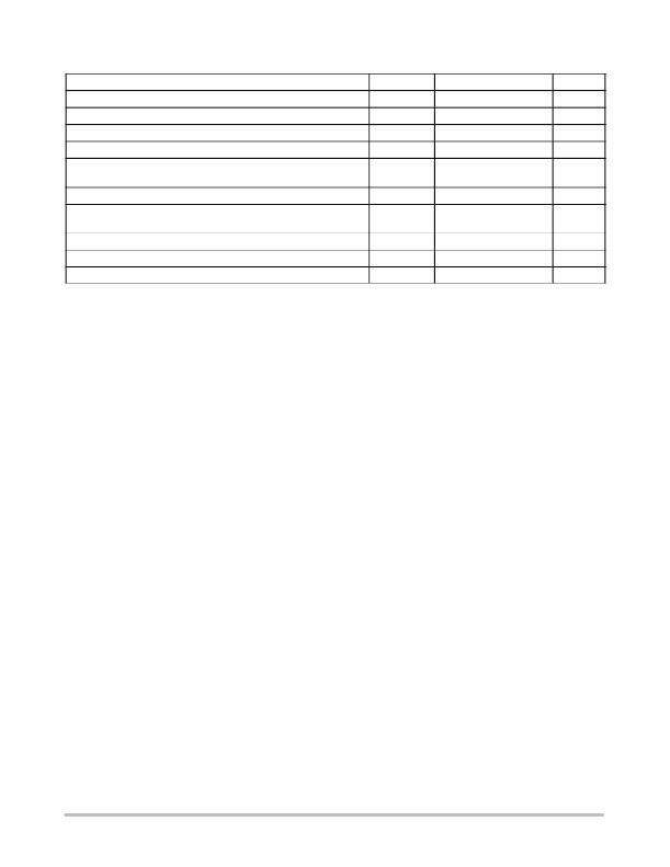
MAXIMUM RATINGS
Rating
Power Supply Voltage (Note 2)
Over Voltage Protection
Human Body Model (HBM) ESD Rating (Note 3)
Machine Model (MM) ESD Rating (Note 3)
Digital Input Voltage
Digital Input Current
Power Dissipation @ T A = +85 ° C
Thermal Resistance Junction?to?Air
8?Pin Flip?Chip Package
Operating Ambient Temperature Range
Operating Junction Temperature Range
Storage Temperature Range
Symbol
V IN
V OUT
ESD HBM
ESD MM
CTRL
P D
R q JA
T A
T J
T stg
Value
7.0
24
2000
200
?0.3 < V IN < V bat +0.3
1.0
150
(Note 6)
?40 to +85
?40 to +125
?65 to +150
Unit
V
V
V
V
V
mA
mW
° C/W
° C
° C
° C
Stresses exceeding Maximum Ratings may damage the device. Maximum Ratings are stress ratings only. Functional operation above the
Recommended Operating Conditions is not implied. Extended exposure to stresses above the Recommended Operating Conditions may affect
device reliability.
1. Maximum electrical ratings are defined as those values beyond which damage to the device may occur at T A = 25 ° C.
2. According to JEDEC standard JESD22?A108B.
3. This device series contains ESD protection and passes the following tests:
Human Body Model (HBM) ± 2.0 kV per JEDEC standard: JESD22?A114 for all pins.
Machine Model (MM) ± 200 V per JEDEC standard: JESD22?A115 for all pins.
4. Latchup Current Maximum Rating: ± 100 mA per JEDEC standard: JESD78.
5. Moisture Sensitivity Level (MSL): 1 per IPC/JEDEC standard: J?STD?020A.
6. For the 8?Pin Flip?Chip CSP Package, the R q JA is highly dependent on the PCB Heatsink area. For example R q JA can be to 195 ° C/W with
50 mm total area and also 135 ° C/W with 500 mm. All the bumps have the same thermal resistance and need to be connected thereby optimizing
the power dissipation.
http://onsemi.com
3
发布紧急采购,3分钟左右您将得到回复。
相关PDF资料
NCP5021MUTXG
IC WHITE LED DVR HV AMB 16-UQFN
NCP5050MTTXG
IC LED DRIVR PHOTO FLASH 10-WDFN
NCP5111DR2G
IC DRIVER HI/LOW SIDE HV 8-SOIC
NCP5304DR2G
IC DRIVER HI/LOW SIDE HV 8-SOIC
NCP5355DG
IC DRVR SYNC BUCK MOSF 12A 8SOIC
NCP5359ADR2G
IC MOSFET GATE DVR DUAL 8-SOIC
NCP5359DR2G
IC GATE DRIVER VR11.1/AMD 8-SOIC
NCP5360RMNR2G
IC DRIVER MOSFET 56QFN
相关代理商/技术参数
NCP502
制造商:ONSEMI 制造商全称:ON Semiconductor 功能描述:80 mA CMOS Low Iq Voltage Regulator in an SC70−5
NCP502 K20PA WAF
制造商:ON Semiconductor 功能描述:
NCP502/D
制造商:未知厂家 制造商全称:未知厂家 功能描述:80 mA CMOS Low Iq Voltage Regulator in an SC70-5
NCP502_07
制造商:ONSEMI 制造商全称:ON Semiconductor 功能描述:80 mA CMOS Low Iq, Low−Dropout Voltage Regulator
NCP5021
制造商:ONSEMI 制造商全称:ON Semiconductor 功能描述:High Voltage White LED Driver with Ambient Light Sensing
NCP5021MUTXG
功能描述:低压差稳压器 - LDO NCP5021 RoHS:否 制造商:Texas Instruments 最大输入电压:36 V 输出电压:1.4 V to 20.5 V 回动电压(最大值):307 mV 输出电流:1 A 负载调节:0.3 % 输出端数量: 输出类型:Fixed 最大工作温度:+ 125 C 安装风格:SMD/SMT 封装 / 箱体:VQFN-20
NCP502ASQ15T1
制造商:ONSEMI 制造商全称:ON Semiconductor 功能描述:80 mA CMOS Low Iq Voltage Regulator in an SC70−5
NCP502ASQ15T1G
制造商:ONSEMI 制造商全称:ON Semiconductor 功能描述:80 mA CMOS Low Iq, Low−Dropout Voltage Regulator